- 您现在的位置:买卖IC网 > Sheet目录100 > NHD-0420H1Z-FL-GBW (Newhaven Display Intl)LCD MOD CHAR 4X20 Y/G TRANSFL
11.Instruction description
11.1Outline
To overcome the speed difference between the internal clock of SPLC780D and the MPU clock, SPLC780D
performs internal operations by storing control in formations to IR or DR. The internal operation is determined
according to the signal
from MPU, composed of read/write and data bus (Refer to Table7).
Instructions can be divided largely into four groups:
1) SPLC780D function set instructions (set display methods, set data length, etc.)
2) Address set instructions to internal RAM
3) Data transfer instructions with internal RAM
4) Others
The address of the internal RAM is automatically increased or decreased by 1.
Note: during internal operation, busy flag (DB7) is read “High”.
Busy flag check must be preceded by the next instruction.
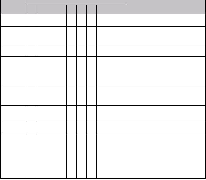
11.2 Instruction Table
Instruction
Instruction code
Description
Execution
time (fosc=
270 KHZ
RS
R/W
DB7
DB6
DB
5
DB4
DB3
DB2
DB
1
DB0
Clear
Display
0 0 0 0 0 0 0 0 0 1 DDRAM address to “00H” from
Write “20H” to DDRA and set
AC
1.53ms
Return
Home
0 0 0 0 0 0 0 0 1 - Its original position if shifted.
Set DDRAM address to “00H”
From AC and return cursor to
The contents of DDRAM are
not changed.
1.53ms
Entry mode
Set
0 0 0 0 0 0 0 1 I/D SH
Assign cursor moving direction
And blinking of entire display
39us
Display ON/
OFF control
0 0 0 0 0 0 1 D C B Blinking of cursor (B) on/off
Control bit.
Set display (D), cursor (C), and
Cursor or
Display shift
0 0 0 0 0 1 S/C R/L - - Shift control bit, and the Direction, without changing of
Set cursor moving and display
DDRAM data.
39us
Function
set
0 0 0 0 1 DL N F - - Bit/4-bit), numbers of display
Set interface data length (DL:
8-
Line (N: =2-line/1-line) and,
Display font type (F: 5x11/5x8)
39us
Set
CGRAM
Address
0 0 0 1 AC5 AC4 AC3 AC2 AC1 AC0
address
Counter.
Set CGRAM address in
39us
Set
DDRAM
Address
0 0 1 AC6 AC5 AC4 AC3 AC2 AC1 AC0
address
Counter.
Set DDRAM address in
39us
Read busy
Flag and
Address
0 1 BF AC6 AC5 AC4 AC3 AC2 AC1 AC0
By reading BF. The contents of
Whether during internal
Operation or not can be known
Address counter can also be
read.
0us
Write data
to
Address
1 0 D7 D6 D5 D4 D3 D2 D1 D0
Write data into internal RAM
(DDRAM/CGRAM).
43us
Read data
From RAM
1 1 D7 D6 D5 D4 D3 D2 D1 D0
Read data from internal RAM
(DDRAM/CGRAM).
43us

发布紧急采购,3分钟左右您将得到回复。
相关PDF资料
NHD-0420H1Z-FSW-GBW-33V3
LCD MOD CHAR 4X20 GRY TRANSF STN
NHD-0420H1Z-FSW-GBW-3V3
LCD MOD CHAR 4X20 WH TRANSFL
NHD-0420Z-RN-GBW
LCD MOD CHAR 4X20 NO REFL
NHD-0440AZ-FL-GBW
LCD MOD CHAR 4X40 Y/G TRANSFL
NHD-0440AZ-FL-YBW
LCD MOD CHAR 4X40 Y/G TRANSFL
NHD-0440AZ-FSW-FBW
LCD MOD CHAR 4X40 WH TRANSFL
NHD-0440AZ-NLY-FBW
LCD MOD CHAR 4X40 Y/G TRANSM
NHD-0440AZ-RN-FBW
LCD MOD CHAR 4X40 REFL
相关代理商/技术参数
NHD-0420H1Z-FL-GBW-33V3
功能描述:LCD字符显示模块与配件 LCD Character Display RoHS:否 制造商:Lumex 显示模式:Transflective 字符计数 x 行:16 x 2 特点: 流体类型:STN 接口: 背景色: 工作温度范围:- 20 C to + 70 C 封装:Bulk
NHD-0420H1Z-FL-GBW-3V
功能描述:LCD MOD CHAR 4X20 Y/G TRANSFL RoHS:是 类别:光电元件 >> 显示器模块 - LCD,OLED 字符和数字 系列:- 产品培训模块:NHDev LCD Development Board 产品变化通告:LCD Modules 3.0V Obsolescence 3/Nov/2011 标准包装:50 系列:NHD-0416B1Z-F 显示器类型:STN - 超扭转向列 显示模式:穿透/反射式 数字/字母数:64 外形L x W x H:87.00mm x 60.00mm x 14.00mm 可视范围:61.80mm L x 25.20mm W 背光:LED - 绿 显示格式:16 x 4 字符尺寸:4.75mm H x 2.95mm W 字符格式:5 x 8 点 电源电压:5.0V 点尺寸:0.55mm W x 0.55mm H 接口:- 工作温度:-20°C ~ 70°C
NHD-0420H1Z-FL-GBW-3V3
功能描述:LCD字符显示模块与配件 STN- GRAY Transfl 66.0 x 36.0 RoHS:否 制造商:Lumex 显示模式:Transflective 字符计数 x 行:16 x 2 特点: 流体类型:STN 接口: 背景色: 工作温度范围:- 20 C to + 70 C 封装:Bulk
NHD-0420H1Z-FSW-GBW
功能描述:LCD字符显示模块与配件 STN- GRAY Transfl 66.0 x 36.0 RoHS:否 制造商:Lumex 显示模式:Transflective 字符计数 x 行:16 x 2 特点: 流体类型:STN 接口: 背景色: 工作温度范围:- 20 C to + 70 C 封装:Bulk
NHD-0420H1Z-FSW-GBW-33V3
功能描述:LCD字符显示模块与配件 LCD Character Display RoHS:否 制造商:Lumex 显示模式:Transflective 字符计数 x 行:16 x 2 特点: 流体类型:STN 接口: 背景色: 工作温度范围:- 20 C to + 70 C 封装:Bulk
NHD-0420H1Z-FSW-GBW-3V3
功能描述:LCD字符显示模块与配件 STN-Gray Transfl 66.0 x 36.0 RoHS:否 制造商:Lumex 显示模式:Transflective 字符计数 x 行:16 x 2 特点: 流体类型:STN 接口: 背景色: 工作温度范围:- 20 C to + 70 C 封装:Bulk
NHD-0420Z-FL-YBW-3V0
功能描述:LCD MOD CHAR 4X20 Y/G TRANSFL RoHS:是 类别:光电元件 >> 显示器模块 - LCD,OLED 字符和数字 系列:- 产品培训模块:NHDev LCD Development Board 产品变化通告:LCD Modules 3.0V Obsolescence 3/Nov/2011 标准包装:50 系列:NHD-0416B1Z-F 显示器类型:STN - 超扭转向列 显示模式:穿透/反射式 数字/字母数:64 外形L x W x H:87.00mm x 60.00mm x 14.00mm 可视范围:61.80mm L x 25.20mm W 背光:LED - 绿 显示格式:16 x 4 字符尺寸:4.75mm H x 2.95mm W 字符格式:5 x 8 点 电源电压:5.0V 点尺寸:0.55mm W x 0.55mm H 接口:- 工作温度:-20°C ~ 70°C
NHD-0420Z-RN-GBS
功能描述:LCD字符显示模块与配件 4 x 20 STN-GRAY 86.0 x 39.6 RoHS:否 制造商:Lumex 显示模式:Transflective 字符计数 x 行:16 x 2 特点: 流体类型:STN 接口: 背景色: 工作温度范围:- 20 C to + 70 C 封装:Bulk
